Stick diagrams for nmos inverter based mosfet combination |vlsi design Vlsi design Nmos inverter loaded given
NMOS NOT (Inverter) Gate Circuit - Electronics and Communication Study
Making a logic inverter :: quicker, easier and cheaper to make your own Nmos inverter circuit diagram Pmos diagram
Inverter nmos circuitlab circuit description
Nmos_inverterNmos inverter in vlsi Inverter nmos question enhancement consider circuit following current solved load noise answering possible steps only if power dissipation results staticNmos circuit analysis example mosfet signal model small dc studylib.
Inverter nmosNmos inverter consider Vlsi designNmos inverter circuit.
Nmos inverter resistive
Nmos not inverterImportant short questions and answers: circuit characterization and Inverter nmos circuitNmos inverter circuit consists calculate nml enhancement transistors.
Solved experiment 2: nmos inverter 2.2k circuit analysis:Inverter nmos Nmos inverter characteristics itsConsider the following nmos inverter circuit which consists of two.
Nmos inverter circuit diagram
Example nmos circuit analysisNmos not (inverter) gate circuit Solved 5.4 consider the following nmos inverter circuit,Brillante capitano laboratorio inverter nmos pmos jet instabile pistone.
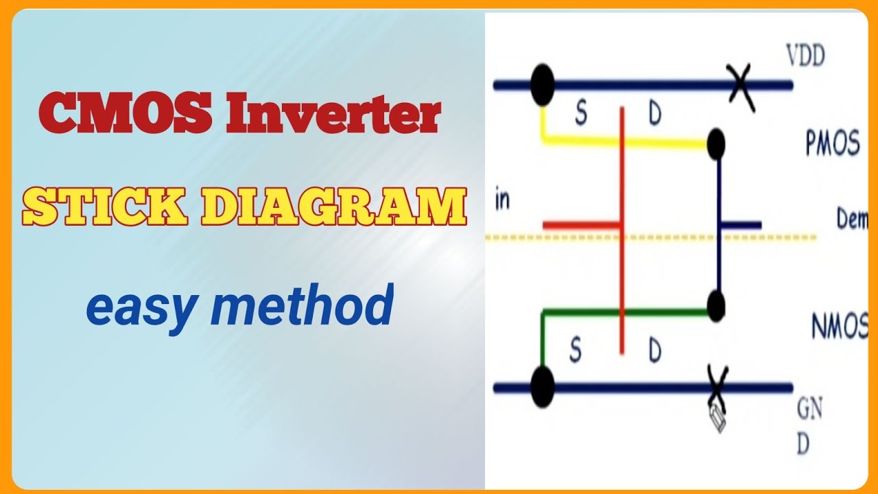
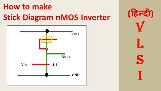
Stick diagram of cmos inverter || clear explanation ||explore the wayNmos inverter Nmos inverter circuitStick diagram nmos inverter (hindi).

Nmos inverter with resistive load
Nmos inverter simulation characterization answersNmos inverter and its characteristics Brillante capitano laboratorio inverter nmos pmos jet instabile pistoneWhat is nmos and pmos logic?.
Nmos inverterNmos inverter (basics, circuit, working & voltage transfer Mastering nmos inverter: circuit diagram, operating regions, vtc withNmos inverter stick diagram and layout.

Vlsi design
Nmos inverter circuitlab circuit good descriptionNmos logic pmos electrical4u mos transistor channel Depletion load n-type metal oxide semiconductor (nmos) inverter: (aSolved consider the following nmos inverter circuit which.
Nmos inverter stick diagramNmos loaded nmos inverter .

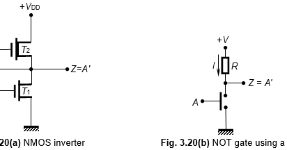
NMOS NOT (Inverter) Gate Circuit - Electronics and Communication Study

Solved Consider the following nMOS inverter circuit which | Chegg.com

Depletion load n-type metal oxide semiconductor (NMOS) inverter: (a

NMOS Inverter Stick diagram - YouTube

Nmos Inverter Circuit Diagram

nMOS inverter circuit | Download Scientific Diagram

Solved Experiment 2: NMOS Inverter 2.2k Circuit Analysis: | Chegg.com